DV/DT Limitation Of SCRs:-
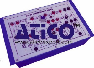
The offered range is known for enhancing the Dv/Dt capability of SCRs to avoid false firing which may be disastrous in some applications. This range is also known for designing and studying various snubber circuits to improve the Dv/Dt capability of thyristors.
Objects:
- Test dv/dt estimation of the SCR
- Compare Dv/Dt capability by gate-cathode terminations
- Compare Dv/Dt capability by gate-cathode biasing (voltage biasing)
- Compare Dv/Dt capability by gate-cathode biasing (current biasing)
- To improve Dv/Dt capability by transistor snubber circuit
- Effect of R.C. snubber circuit on Dv/Dt capability
- Study of different scheme of R.C. Snubber circuit on Dv/Dt capability
Built in parts:
- 300 V D.C. at 250 mA, power supply internally connected
- Thyristor switch for applying sudden voltage on the SCR under experiment
- The SCR under experiment
- Resistance for gate-cathode termination
- Silicon diode
- Transistorized snubber circuit
- Two schemes for R-C snubber circuits
- Visual indication to indicate SCR firing
- Adequate no. of other electronic components
- Mains ON/OFF switch, fuse and jewel light
Specifications:
- The unit is operative on 230 V ±10% at 50 Hz A.C. mains
- Adequate no. of patch cords stackable 4 mm spring loaded plug length ½ meter
- Good quality, reliable terminal/sockets are provided at appropriate places on panel for connections/ observation of waveforms
- Strongly supported by detailed operating instructions, giving details of object, theory, design procedures, report suggestions and book references
- Weight: 3 kg. (approx.)
- Dimension: W 340 x H 110 x D 210


